This post is part of a 4-part series on physics-based modeling of the MOS capacitor.
- MOS capacitor derivation
- Gauss's Law as used in MOS derivations
- MOS surface potential equation
- Automated drawing of the MOS band diagram
1.0 Introduction 
The band-bending that occurs in the semiconductor of an MOS device is quantified as the surface potential, $\psi_s$. It is related to the applied gate-body bias by the "surface potential equation" (SPE), which is derived by combining the following items. (For a brief discussion of band-bending see Section 3.0 of the MOSCAP derivation notebook.)
- Two applications of Gauss's Law (discussed here).
- The assumption that the oxide is charge free.
- The potential balance equation.
Each of the above three items are explained in further detail below. Afterward, they are combined to produce the SPE.
2.0 Components of the SPE
2.1 Result #1: Gauss's Law
The results of the two applications of Gauss's Law are:
$$\begin{aligned} \epsilon_s \cdot E_s - \epsilon_{ox} \cdot E_{ox} &= Q_o' + Q_{it}' \\ -\epsilon_s \cdot E_s &= Q_s' \end{aligned}$$Substituting the second equation into the first equation gives an expression in terms of two charges per unit area and the oxide field.
$$\begin{aligned} -(Q_o' + Q_{it}' + Q_s') &= \epsilon_{ox} \cdot E_{ox} \end{aligned}$$2.2 Result #2: oxide without bulk charge
If there is no charge within the oxide, the electric field must be constant. This can be proven by considering Gauss's Law in a one-dimensional charge free region (e.g., $dE/dy = 0$ so $E$ must be a constant). Therefore, the electric field, $E_{ox}$, is simply the oxide potential drop divided by the oxide thickness.
$$\begin{aligned} E_{ox} &= \frac{\psi_{ox}}{t_{ox}} \end{aligned}$$2.3 Result #3: potential balance equation
The potential balance equation comes from performing a KVL around the MOS band diagram with the local vacuum level ($E_{VAC}$) included. While manuevering clockwise starting at the metal's Fermi level, a rise is taken to be positive and a drop is considered negative.
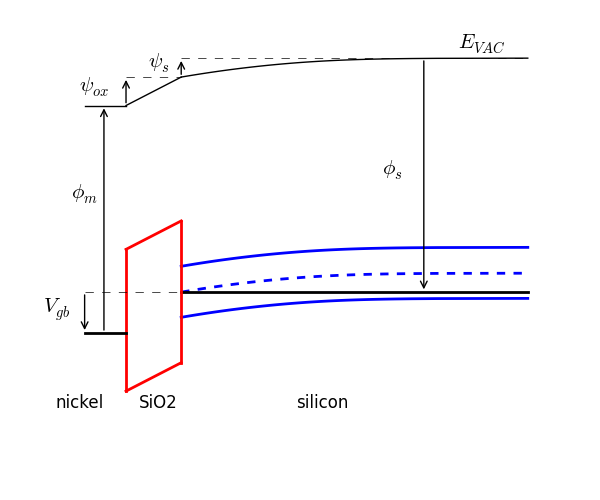
$\phi_{ms} = \phi_m - \phi_s$ is the difference between the metal and semiconductor workfunctions, which leads to a more recognizable form of the above.
$$\begin{aligned} V_{gb} &= \psi_{ox} + \psi_s + \phi_{ms} \end{aligned}$$3.0 The SPE 
Substituting Result #2 into Result #1 gives:
$$\begin{aligned} -(Q_o' + Q_{it}' + Q_s') &= \epsilon_{ox} \cdot \frac{\psi_{ox}}{t_{ox}} \\ &= C_{ox}' \cdot \psi_{ox} \end{aligned}$$The quantity $\epsilon_{ox} / t_{ox}$ is hereafter replaced with $C_{ox}'$, which is the oxide capacitance per unit area. Often, it is referred to as the oxide capacitance density. After making this simplification, $\psi_{ox}$ can be found.
$$\begin{aligned} \psi_{ox} &= \frac{-(Q_o' + Q_{it}' + Q_s')}{C_{ox}'} \\ \end{aligned}$$Inserting the above expression for $\psi_{ox}$ into the Result #3 and simplifying gives the SPE.
$$\begin{aligned} V_{gb} &= \psi_s + \phi_{ms} + \frac{-(Q_o' + Q_{it}' + Q_s')}{C_{ox}'} \end{aligned}$$A more commonly seen version is in terms of the flatband voltage, $V_{fb}$. This is simply the value of $V_{gb}$ when $\psi_s=0$. When $\psi_s$ is zero, $Q_s'$ is also zero (see MOS derivation), so two of the terms in the SPE drop out. The quantity $Q_{it}'(\psi_s=0)$ is denoted $Q_{it0}$.
$$\begin{aligned} V_{fb} &= \phi_{ms} - \frac{Q_o' + Q_{it0}'}{C_{ox}'} \end{aligned}$$The above can be substituted back into the SPE so that it incorporates a flatband voltage term.
$$\begin{aligned} V_{gb} &= \psi_s + V_{fb} - \frac{Q_{it}' - Q_{it0}' + Q_s'}{C_{ox}'} \end{aligned}$$A more recognizable form of the SPE that is often found in textbooks occurs when $Q_{it}$ is zero.
$$\begin{aligned} V_{gb} &= \psi_s + V_{fb} - \frac{Q_s'}{C_{ox}'} \end{aligned}$$
Comments !