This post is part of a 4-part series on physics-based modeling of the MOS capacitor.
- MOS capacitor derivation
- Gauss's Law as used in MOS derivations
- MOS surface potential equation
- Automated drawing of the MOS band diagram
1.0 Introduction 
There are two applications of Gauss's Law used in MOS derivations for computing the surface potential equation (SPE). One of the applications is also used in the formulation of semiconductor charge per unit area from the surface field that is found during the solution of Poisson's equation. Some background is given before they are discussed.
2.0 Simplified one-dimensional MOS system 
The primary assumption is that of an oxide whose oxide-related defects are assumed to only exist at the oxide/semiconductor interface. These defects are identified with the $Q_o'$ and $Q_{it}'$ variables. The former is fixed charge that does not change in magnitude with band-bending. The latter is from interface states, whose occupation does change with band-bending.
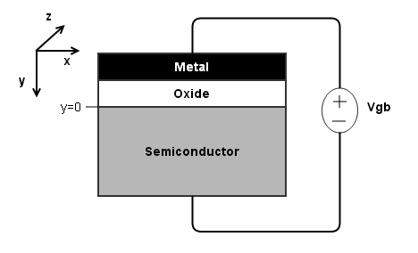
The secondary assumption is that the metal, oxide, and semiconductor layers each exist as uniform planes that stretch to infinity in the x and z directions. The latter assumption permits one to apply Gauss's Law at some arbitrary location and have its result be valid at any location.

3.0 Gauss's Law 
In differential form, Gauss's Law relates the divergence of electric field to charge density.
$$\begin{aligned} \nabla \cdot \overrightarrow{E} &= \frac{\rho}{\epsilon} \end{aligned}$$When a potential is applied between the metal and semiconductor layers, the electric field is one dimensional because of the uniform planarity mentioned above. $\overrightarrow{E}$ is now only composed of the y-direction component, $E_y$, where the subscript is dropped going forward.
$$\begin{aligned} \frac{dE}{dy} &= \frac{\rho}{\epsilon} \\ \end{aligned}$$A one-dimensional application of Gauss's Law from point A to point B gives the following result. $Q_{\mbox{enclosed}}$ is the total charge contained in the region between A and B. The subscripts A and B mean the quantity is to be evaluated at either A or B.
$$\begin{aligned} \int_A^B \epsilon dE &= \int_A^B \rho dy \\ \epsilon_B \cdot E_B - \epsilon_A \cdot E_A &= Q_{\mbox{enclosed}} \end{aligned}$$In the below applications of Gauss's Law it is always chosen that location A is above location B in the cross-section displayed above (stated mathematically, $y_A < y_B$).
4.0 Gauss's Law as applied to create the SPE
4.1 Result #1
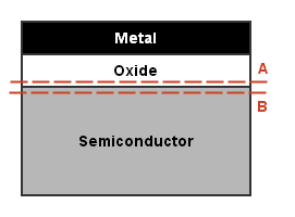
Consider the region between the red dashed lines below. Let the top/bottom lines be just above/below the oxide/semiconductor interface. That is, let the top be at $y_A=0^-$ and the bottom at $y_B=0^+$. With these constraints, the region between these lines contains no semiconductor charge and only includes fixed/interface charge.

Going forward, subscripts A and B are replaced with 'ox' (oxide) and 's' (semiconductor surface). Applying Gauss's Law in the $y$-direction at any $(x, z)$ location gives:
$$\begin{aligned} \epsilon_s \cdot E_s - \epsilon_{ox} \cdot E_{ox} &= Q_o' + Q_{it}' \end{aligned}$$$Q_o'$ and $Q_{it}'$ are charges per unit area. The "prime" superscript is what indicates that this quantity is a charge per unit area. The units come out this way because $\rho$ is charge per unit volume and is integrated with respect to distance.
Note: in the absence of oxide charge, $\epsilon_s \cdot E_s = \epsilon_{ox} \cdot E_{ox}$.
Both $Q_o'$ and $Q_{it}'$ are the same regardless of where Gauss's Law is applied due to the planar homogeneity assumed above.
4.2 Result #2
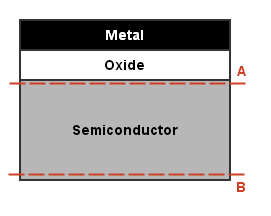
The following figure shows a dashed line drawn just below the interface, and another dashed line drawn at the bottom of the semiconductor. Let the top be at $y_A=0^+$ (the semiconductor surface, denoted with subscript 's') and the bottom at the end of the semiconductor bulk where electric field has decayed to zero. With these constraints the region between the two lines only contains semiconductor charge.

Therefore, Gauss's Law gives:
$$\begin{aligned} -\epsilon_s \cdot E_s &= Q_s' \end{aligned}$$$Q_s'$ is the total semiconductor charge per unit area. As with $Q_o'$ and $Q_{it}'$, it is the same regardless of the location chosen to apply Gauss's Law.
Comments !