This post is part of a 4-part series on physics-based modeling of the MOS capacitor.
- MOS capacitor derivation
- Gauss's Law as used in MOS derivations
- MOS surface potential equation
- Automated drawing of the MOS band diagram
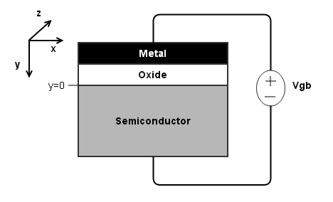
1.0 Introduction 
The MOS capacitor's band diagram can be drawn using results from the one-dimensional solution of Poisson's equation. The accuracy of the resulting band diagram is only as good as the approximations used in the analysis. Zero gate leakage is assumed.
This notebook draws the band diagram for the nickel-SiO2-Si system at an arbitrary gate-bulk bias. It uses published conduction/valence band offsets (CBO/VBO) for SiO2 on silicon [1]. Other insulators can be substituted if their CBO/VBO are known, either from published measurements or by resorting to the affinity rule. The CBO/VBO values have no effect on the computed band-bending since gate leakage is ignored, so even fictional values can be input. CBO/VBO are only included so that the insulator can be outlined while showing the effect of $\psi_{ox}$.
The y-axis of the resulting band diagram will be in eV. However, the values should be interpreted as being relative to the semiconductor's neutral bulk valence band level, $E_v(y\rightarrow\infty)$.
1.1 A brief primer on band-bending
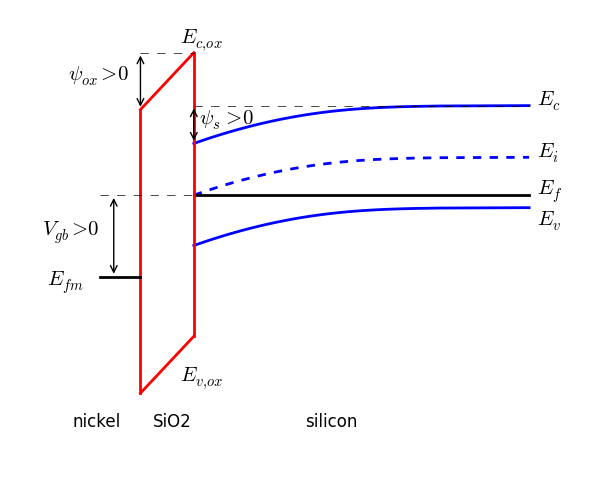
The amount of band-bending in the semiconductor at an arbitrary depth is quantified as potential, $\psi$. The surface potential, $\psi_s$, is the total band-bending from the neutral bulk to the oxide/semiconductor interface.
- Band-bending is positive when a band is bent downward.
- Band-bending is negative when a band is bent upward.
Below is an image showing band-bending in an MOS device when $V_{gb}$, $\psi_{ox}$, and $\psi_s$ are all positive.
2.0 Constants and utility functions
import numpy as np
import matplotlib.pyplot as plt
import matplotlib as mpl
from scipy.integrate import quad
# The 'inline' statement keeps the plot windows from showing up as
# independent windows.  Instead, they show up in the notebook.
%matplotlib inline
# make all lines have this thickness by default
mpl.rcParams['lines.linewidth'] = 2
# set a default figure size
mpl.rcParams['figure.figsize'] = (8, 5)
# -----------------------
# user-defined settings
# -----------------------
T = 300 # lattice temperature, Kelvin
tox = 20e-9 * 100 # 50 nm oxide converted to cm
Nd = 1e16 # donor doping concentration, # / cm^3
Na = 1e17 # acceptor doping concentration, # / cm^3
CBO = 3.5 # SiO2/Si conduction band offset, eV
VBO = 4.4 # SiO2/Si valence band offset, eV

# -----------------------
# physical constants
# -----------------------
e0 = 8.854e-14 # permittivity of free space, F / cm
q = 1.602e-19 # elementary charge, Coulombs
k = 8.617e-5 # Boltzmann constant, eV / K

# -----------------------
# material parameters
# -----------------------
es = 11.7 # relative permittivity, silicon
eox = 3.9 # relative permittivity, SiO2
chi_s = 4.17 # electron affinity, silicon, eV
phi_m = 5.01 # work function, nickel, eV
# bandgap, silicon, eV
Eg = 1.17 - 4.73e-4 * T ** 2 / (T + 636.0)
# effective valence band DOS, silicon, # / cm^3
Nv = 3.5e15 * T ** 1.5
# effective conduction band DOS, silicon, # / cm^3
Nc = 6.2e15 * T ** 1.5

def solve_bisection(func, target, xmin, xmax):
    """
    Returns the independent value x satisfying func(x)=value.
    - uses the bisection search method
      https://en.wikipedia.org/wiki/Bisection_method

    Arguments:
        func - callable function of a single independent variable
        target - the value func(x) should equal
        [xmin, xmax] - the range over which x can exist
    """
    tol = 1e-10 # when |a - b| <= tol, quit searching
    max_iters = 1e2 # maximum number of iterations
    a = xmin
    b = xmax
    cnt = 1
    # before entering while(), calculate Fa
    Fa = target - func(a)
    c = a

    # bisection search loop
    while np.abs(a - b) > tol and cnt < max_iters:
        cnt += 1
        # make 'c' be the midpoint between 'a' and 'b'
        c = (a + b) / 2.0
        # calculate at the new 'c'
        Fc = target - func(c)

        if Fc == 0:
            # 'c' was the sought-after solution, so quit
            break
        elif np.sign(Fa) == np.sign(Fc):
            # the signs were the same, so modify 'a'
            a = c
            Fa = Fc
        else:
            # the signs were different, so modify 'b'
            b = c

    if cnt == max_iters:
        print('WARNING: max iterations reached')

    return c

# -----------------------
# dependent calculations
# -----------------------
# intrinsic carrier concentration, silicon, # / cm^3
ni = np.sqrt(Nc * Nv) * np.exp(-Eg / (2 * k * T))
# Energy levels are relative to one-another in charge expressions.
# - Therefore, it is OK to set Ev to a reference value of 0 eV.
# Usually, energy levels are given in Joules and one converts to eV.
# - I have just written each in eV to save time.
Ev = 0 # valence band energy level
Ec = Eg # conduction band energy level
Ei = k * T * np.log(ni / Nc) + Ec # intrinsic energy level
phit = k * T # thermal voltage, eV
# get the Fermi level in the bulk where there is no band-bending
n = lambda Ef: Nc * np.exp((-Ec + Ef) / phit)
p = lambda Ef: Nv * np.exp((Ev - Ef) / phit)
func = lambda Ef: p(Ef) - n(Ef) + Nd - Na
Ef = solve_bisection(func, 0, Ev, Ec)
# compute semiconductor work function (energy from vacuum to Ef)
phi_s = chi_s + Ec - Ef
# flatband voltage and its constituent(s)
# - no defect-related charges considered
phi_ms = phi_m - phi_s # metal-semiconductor workfunction, eV
Vfb = phi_ms # flatband voltage, V
# oxide capacitance per unit area, F / cm^2
Coxp = eox * e0 / tox
# if both Nd and Na are zero, then make one slightly higher
# calculate effective compensated doping densities
# - assume complete ionization
if Na > Nd:
    Na = Na - Nd
    Nd = 0
    device_type = 'nMOS'
else:
    Nd = Nd - Na
    Na = 0
    device_type = 'pMOS'
# -----------------------
# define the SPE
# -----------------------
# compute equilibrium carrier concentrations
n_o = Nc * np.exp((-Ec + Ef) / phit)
p_o = Nv * np.exp((Ev - Ef) / phit)
# define the charge function so it can be used in the SPE
f = lambda psis: psis * (Na - Nd) \
  + phit * p_o * (np.exp(-psis / phit) - 1) \
  + phit * n_o * (np.exp(psis / phit) - 1)
Qs = lambda psis: -np.sign(psis) * np.sqrt(2 * q * e0 * es * f(psis))
SPE = lambda psis: Vfb + psis - Qs(psis) / Coxp
# define the electric field for use in computing y(psi)
E = lambda psi: np.sign(psi) * np.sqrt(2 * q / (es * e0) * f(psi))
3.0 Derivation of $\psi(y)$ 
The first step to obtaining semiconductor potential ($\psi$) as a function of distance ($y$) from the oxide-semiconductor interface is to have an expression for electric field. The semiconductor's electric field is known from analysis of Poisson's equation. Only the highlights of the derivation are shown below.
$$\begin{aligned} \frac{d^2\psi}{dy^2} &= -\frac{\rho}{\epsilon_s} \\ \rightarrow \frac{1}{2} \frac{dE^2}{d\psi} &= -\frac{\rho}{\epsilon} \\ \int_{E(y=0)}^{E(y)} dE^2 &= -\frac{2}{\epsilon} \int_{\psi(y=0)}^{\psi(y)} \rho d\psi \end{aligned}$$The resulting $E$ is:
$$\begin{aligned} E &= \mbox{sign}(\psi) \sqrt{\frac{2q}{\epsilon_s} f(\psi)} \\ f(\psi) &= \phi_t p_o \left(e^{-\psi/\phi_t} - 1 \right) + \phi_t n_o \left(e^{\psi/\phi_t} - 1 \right) \\ & + \psi \left(N_a - N_d\right) \end{aligned}$$Now, a relationship between $E$ and $\psi$ is known. Obtaining the $y$ value at each $(\psi, E)$ pair comes from the one-dimensional potential/field relationship, $E = -dV/dy$. Rearranging the derivative and integrating gives a function for $y$. The resulting integral has no closed-form result and so must be discretely integrated. The subscript 'a' in $y_a$ and $\psi_a$ just means 'arbitrary' and is only added to avoid having the variable of integration appear in the integral's limits.
$$\begin{aligned} \int_0^{y_a} dy &= -\int_{\psi_s}^{\psi_a} \frac{d\psi}{E} \\ y_a &= \int_{\psi_a}^{\psi_s} \frac{d\psi}{\mbox{sign}(\psi) \sqrt{\frac{2q}{\epsilon_s} f(\psi)}} \end{aligned}$$The band diagram function will:
- Define/compute the surface potential ($\psi_s$), gate-bulk voltage ($V_{gb}$), and oxide potential ($\psi_{ox}$).
- Create a new variable ($\psi$) that ranges from $\psi_s$ to near-zero.
- At each $\psi$ value, numerically integrate the right-hand side of the $y$ expression to obtain the corresponding value of $y$.
A function that performs the numerical integration is defined first so that it can be called during the band diagram drawing routine.
3.1 $y$-computation functions
# -----------------------
# y-computation functions
# -----------------------
# this is the integrand needed to compute y
integrand_y = lambda psi: 1 / E(psi)

def compute_y_vs_psi(psis):
    """
    This function creates a 'psi' variable ranging from psis to ~zero.
    It then computes the y-values corresponding to every value in psi.

    psis is the surface potential and must be a scalar constant.
    """
    # handle the flatband case
    if psis == 0:
        y = np.linspace(0, 150, 101) * 1e-7 # convert nm to cm
        psi = 0 * y
        return y, psi
    # (1) let semiconductor potential range from psis to near-zero
    # - could construct psi linearly and have a coarse y as psi -> 0
    # - could construct psi log-spaced to make y more evenly spaced
    # - solution: do a mixture
    psi1 = np.linspace(psis, psis * 0.5, 21) # linear spacing near y=0
    psi2 = np.logspace(                      # log spacing toward bulk
        np.log10(np.abs(psis * 0.5)),
        np.log10(np.abs(psis * 1e-3)),
        101
    )
    if psis < 0:
        psi2 = -1 * psi2
    # combine the arrays, but leave out the common point (psis * 0.5)
    psi = np.hstack((psi1, psi2[1:]))
    # (2) call compute_y() at every value in psi
    # collect the returned y-values in an array
    y = np.array([])
    for value in psi:
        y_current, error = quad(integrand_y, value, psis)
        y = np.hstack((y, y_current))
    return y, psi
4.0 Computed band diagram
# -----------------------
# choose a potential to plot
# -----------------------
# psis = Ev - Ef                    # (very) strong accumulation
# psis = 0                          # flatband
# psis = Ei - Ef                    # weak inversion
# psis = 2 * (Ei - Ef)              # strong inversion
psis = 2 * (Ei - Ef) + 3 * phit   # stronger inversion
# psis = Ec - Ef                    # (very) strong inversion
# psis = solve_bisection(           # zero gate-bulk bias
#     SPE, 0, Ev - Ef, Ec - Ef
# )

# compute the corresponding Vgb value
Vgb = SPE(psis)

# create figure, label axes, turn grid on
plt.figure(1)
plt.xlabel('y (nm)', fontsize=14)
plt.ylabel('relative to bulk valence band (eV)', fontsize=14)
plt.grid(True)

# get psiox from the potential balance equation (see SPE derivation)
psiox = Vgb - psis - phi_ms

# construct the psi vs y curve
y, psi = compute_y_vs_psi(psis)
# y and tox are in cm, so convert to nm
y = y / 100 * 1e9
toxnm = tox / 100 * 1e9

# plot the conduction/intrinsic/valence bands
plt.plot(y, Ev - psi, 'b')
plt.plot(y, Ei - psi, 'b--')
plt.plot(y, Ec - psi, 'b')

# plot the fermi level
plt.plot(y, 0 * y + Ef, 'k')

# plot the SiO2 bands
plt.plot([0, 0], [Ev - psis - VBO, Ec - psis + CBO], 'r')
plt.plot(
    [-toxnm, -toxnm],
    [Ev - psis - VBO - psiox, Ec - psis + CBO - psiox],
    'r'
)
plt.plot([-toxnm, 0], [Ev - psis - VBO - psiox, Ev - psis - VBO], 'r')
plt.plot([-toxnm, 0], [Ec - psis + CBO - psiox, Ec - psis + CBO], 'r')

# plot the gate's Fermi level
plt.plot(
    [-toxnm - 15, -toxnm],
    [Ef - phi_ms - psis - psiox, Ef - phi_ms - psis - psiox],
    'k'
)

print('Vgb = %0.4g, psiox = %0.4g, psis = %0.4g' % (Vgb, psiox, psis))

5.0 Related: Plotting $\rho(y)$
The charge density, $\rho$, is a function of depth and can now be plotted using the $\psi$ vs $y$ relationship computed above. Complete dopant ionization is assumed.
$$\begin{aligned} \rho(y) &= q \left(p(y) - n(y) + N_d - N_a\right) \\ &= q \left(p_o e^{\psi(y)/\phi_t} - n_o e^{\psi(y)/\phi_t} + N_d - N_a\right) \end{aligned}$$In the below plot, one can observe that the majority carrier concentration approaches the background doping level as $y$ becomes large. $\rho$ may not approach near-zero since $y$ was not computed when $\psi$ is extremely close to zero (see construction of $\psi$ in compute_y_vs_psi(psis)).
# define the components of rho
n = n_o * np.exp(psi / phit)
p = p_o * np.exp(-psi / phit)
rho_by_q = p - n + Nd - Na

# plot the components of rho
plt.figure(2)
plt.xlabel('y (nm)', fontsize=14)
plt.ylabel('(# / cm$^3$)', fontsize=14)
plt.grid(True)
plt.semilogy(y, n, label='n', linewidth=2)
plt.semilogy(y, p, label='p', linewidth=2)
if device_type == 'nMOS':
    plt.semilogy(y, Na + 0 * y, label='$N_a$')
else:
    plt.semilogy(y, Nd + 0 * y, label='$N_a$')
plt.legend(loc='best', prop={'size': 16})

# show magnitude of rho on a log scale
plt.figure(3)
plt.xlabel('y (nm)', fontsize=14)
plt.ylabel('$|\\rho/q|$ (# / cm$^3$)', fontsize=16)
plt.grid(True)
tmp = plt.semilogy(y, np.abs(rho_by_q), label='$\\rho/q$')


Download this post's IPython notebook here.
Comments !