This post is part of a 4-part series on physics-based modeling of the MOS capacitor.
- MOS capacitor derivation
- Gauss's Law as used in MOS derivations
- MOS surface potential equation
- Automated drawing of the MOS band diagram
1.0 Introduction
This notebook presents the mathematical derivation of the electrical characteristics belonging to the MOS capacitor. Although this topic is well-covered in numerous books and technical papers, the mathematics must be implemented in code by the reader. While this is a useful and highly recommended exercise, I thought it might be nice to leverage the IPython notebook's capability to simultaneously display discussion, typset math, and code.
This notebook assumes the reader is familiar with basic sold-state physics concepts such as band diagrams, carrier statistics, and Poisson's equation.
1.1 Model assumptions
- MOS material system is nickel - SiO2 - silicon
- perfect insulator (zero bulk/interface state density)
- thick insulator so that quantum confinement can be ignored
- thick substrate such that the electric field deep in the bulk approaches zero
- non-degenerate substrate doping
- non-freezeout temperature range such that Maxwell-Boltzmann statistics apply
1.2 Coordinate system and cross section
The MOS capacitor's electrical characteristics are derived by analyzing a fictionalized geometrical representation. It is assumed that the metal, oxide, and semiconductor layers each exist as planes with uniform characteristics that stretch to infinity in the x and z directions. This assumption permits one to solve Poisson's equation in one-dimension (the y-direction) at an arbitrary x, z location and obtain the same result as solving it in another location.
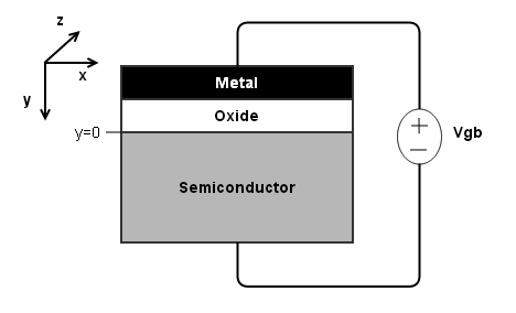
Due to the one-dimensional analysis, all derived quantities' units have area in the denominator (each quantity is in "per unit area"). A typical MOS capacitor with gate area $A$ will have electrodes on the top of the gate and at the bottom of the substrate. If one is measuring capacitance, then to compare the measured result to the calculated value one would have to either divide the measured capacitance by $A$ or multiply the calculated value by $A$.
Furthermore, it is assumed that the semiconductor layer is infinitely thick. This provides a convenient boundary condition where potential and field decay to zero. More on this topic is discussed in Section 6.0 when Poisson's equation is solved.
1.3 Doping limitations
Some of the expressions in this notebook are exact, while some of the expressions are derived using the charge sheet approximation. The code containing the latter group of expressions will fail if the doping is set to zero or if acceptor doping density is equal to donor doping density. This is because the charge sheet approximation assumes there is a net doping density above the intrinsic level. Therefore, some plots will not appear or will contain curves that do not cover the entire independent range, both usually caused by NaN values.
Also, the degenerate doping case is not handled. To handle that case one must resort to Fermi-Dirac carrier statistics and include a bandgap-narrowing term, or just reformulate the analysis to consider quantum-mechanical effects.
1.4 Code
The code contained in this notebook was tested successfully in Python v2.7.5 and v3.4.2. Numpy, scipy, and matplotlib modules are required. For Windows users, it is suggested to use WinPython or Pythonxy. At the time of this writing, only the former has Python3 versions available.
All code can be copied into a single Python script provided each cell is included sequentially. All plots shown in this notebook will appear.
2.0 Constants and utility functions
The following code blocks contain functions and variables that are commonly used. Constants are defined here so that they are available in the Python namespace later on. Most, if not all, of the material constants come from the Ioffe semicondudctor properties archive [1].
import numpy as np
import matplotlib.pyplot as plt
from scipy.integrate import quad
# The 'inline' statement keeps the plot windows from showing up as
# independent windows.  Instead, they show up in the notebook.
%matplotlib inline
# set a default figure size
mpl.rcParams['figure.figsize'] = (8, 5)
# -----------------------
# user-defined settings
# -----------------------
T = 300 # lattice temperature, Kelvin
tox = 50e-9 * 100 # 50 nm oxide converted to cm
Nd = 1e16 # donor doping concentration, # / cm^3
Na = 1e17 # acceptor doping concentration, # / cm^3

# -----------------------
# physical constants
# -----------------------
e0 = 8.854e-14 # permittivity of free space, F / cm
q = 1.602e-19 # elementary charge, Coulombs
k = 8.617e-5 # Boltzmann constant, eV / K

# -----------------------
# material parameters
# -----------------------
es = 11.7 # relative permittivity, silicon
eox = 3.9 # relative permittivity, SiO2
chi_s = 4.17 # electron affinity, silicon, eV
phi_m = 5.01 # work function, nickel, eV
# bandgap, silicon, eV
Eg = 1.17 - 4.73e-4 * T ** 2 / (T + 636.0)
# effective valence band DOS, silicon, # / cm^3
Nv = 3.5e15 * T ** 1.5
# effective conduction band DOS, silicon, # / cm^3
Nc = 6.2e15 * T ** 1.5
An indicator function proves to be useful when implementing expressions prone to 0/0 conditions. The below is formulated to "indicate" that x is zero by returning unity. Otherwise, it returns zero.
$$\begin{aligned} I(x) &= 1 - |\mbox{sign}(x)| \end{aligned}$$The $\mbox{sign}$ function returns $1/0/-1$ if $x$ is positive/zero/negative. It is available in the Python module numpy and is often referred to as $\mbox{signum}$ in other computational tools.
A smoothing function is needed when it is desired that a function smoothly transitions to near-zero [2]. This can be useful to prevent a function from changing sign. In the following functions, the parameter $\varepsilon$ controls how quickly the function $f$ transitions toward zero. Two versions are written: $S_p$ ensures $f$ stays positive, and $S_n$ ensures $f$ stays negative.
$$\begin{aligned} S_p(f) &= \frac{f + \sqrt{f^2 + 4\varepsilon^2}}{2} \\ S_n(f) &= \frac{f - \sqrt{f^2 + 4\varepsilon^2}}{2} \end{aligned}$$Note that when $f^2 \ll 4\varepsilon^2$, then $S_p \approx \varepsilon$ and $S_n \approx -\varepsilon$. This means that the minimum value of $|f|$ is clamped to $\varepsilon$, which must be carefully chosen.
# create an indicator function
# - this function is unity only when x is zero; else, it returns zero
I = lambda x: 1 - np.abs(np.sign(x))

# create smoothing functions
# - smoothly transitions to near-zero as f approaches zero
# - eps is the minimum value |f| reaches
def Sp(f, eps=1e-3):
    return (f + np.sqrt(f ** 2 + 4 * eps ** 2)) / 2.0
def Sn(f, eps=1e-3):
    return (f - np.sqrt(f ** 2 + 4 * eps ** 2)) / 2.0
In this notebook, comments involving the phrase "numerical solution" appear. This refers to solving a transcendental function using an iterative approach, which is stated more mathematically as finding the value, $x_0$, that satisfies $f(x_0) = 0$. The most flexible iterative approach is the midpoint method, which continually bisects a range of independent values that is assumed to contain $x_0$. Newton's method is an alternative (and faster) approach, but is not employed since it requires the user to compute the derivative of $f(x)$.
def solve_bisection(func, target, xmin, xmax):
    """
    Returns the independent value x satisfying func(x)=value.
    - uses the bisection search method
      https://en.wikipedia.org/wiki/Bisection_method

    Arguments:
        func - callable function of a single independent variable
        target - the value func(x) should equal
        [xmin, xmax] - the range over which x can exist
    """
    tol = 1e-10 # when |a - b| <= tol, quit searching
    max_iters = 1e2 # maximum number of iterations
    a = xmin
    b = xmax
    cnt = 1
    # before entering while(), calculate Fa
    Fa = target - func(a)
    c = a

    # bisection search loop
    while np.abs(a - b) > tol and cnt < max_iters:
        cnt += 1
        # make 'c' be the midpoint between 'a' and 'b'
        c = (a + b) / 2.0
        # calculate at the new 'c'
        Fc = target - func(c)

        if Fc == 0:
            # 'c' was the sought-after solution, so quit
            break
        elif np.sign(Fa) == np.sign(Fc):
            # the signs were the same, so modify 'a'
            a = c
            Fa = Fc
        else:
            # the signs were different, so modify 'b'
            b = c

    if cnt == max_iters:
        print('WARNING: max iterations reached')

    return c
With all the material constants assigned only some dependent calculations are required to complete the set up.
# -----------------------
# dependent calculations
# -----------------------
# intrinsic carrier concentration, silicon, # / cm^3
ni = np.sqrt(Nc * Nv) * np.exp(-Eg / (2 * k * T))
# Energy levels are relative to one-another in charge expressions.
# - Therefore, it is OK to set Ev to a reference value of 0 eV.
# Usually, energy levels are given in Joules and one converts to eV.
# - I have just written each in eV to save time.
Ev = 0 # valence band energy level
Ec = Eg # conduction band energy level
Ei = k * T * np.log(ni / Nc) + Ec # intrinsic energy level
phit = k * T # thermal voltage, eV
# get the Fermi level in the bulk where there is no band-bending
n = lambda Ef: Nc * np.exp((-Ec + Ef) / phit)
p = lambda Ef: Nv * np.exp((Ev - Ef) / phit)
func = lambda Ef: p(Ef) - n(Ef) + Nd - Na
Ef = solve_bisection(func, 0, Ev, Ec)
# compute semiconductor work function (energy from vacuum to Ef)
phi_s = chi_s + Ec - Ef
# flatband voltage and its constituent(s)
# - no defect-related charges considered
phi_ms = phi_m - phi_s # metal-semiconductor workfunction, eV
Vfb = phi_ms # flatband voltage, V
# oxide capacitance per unit area, F / cm^2
Coxp = eox * e0 / tox
# calculate effective compensated doping densities
# - assume complete ionization
if Na > Nd:
    Na = Na - Nd
    Nd = 0
    device_type = 'nMOS'
else:
    Nd = Nd - Na
    Na = 0
    device_type = 'pMOS'
3.0 Band-bending and surface potential
All bias-dependent expressions in this work make use of the concept of band-bending, which is denoted by the variable $\psi$. Furthermore, the band-bending from the neutral semiconductor bulk to the semiconductor-insulator surface is termed surface potential ($\psi_s$).
- Band-bending is positive when a band is bent downward (excess electrons are induced).
- Band-bending is negative when a band is bent upward (excess holes are induced).
Below is an image showing band-bending in an MOS device when $V_{gb}$, $\psi_{ox}$, and $\psi_s$ are all positive.
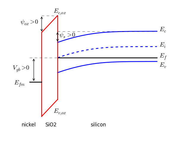
Note: The above surface potential definition follows the style of Y. Tsividis [3], which is in contrast to works that define surface potential to be the difference between the Fermi level in the neutral bulk with the intrinsic level at the surface (e.g., [4]). The two definitions only differ by a constant (the fermi potential, $\phi_f$).
4.0 Charge density
The four charges present in the semiconductor bulk are:
- free holes ($p$, positive charge)
- free electrons ($n$, negative charge)
- ionized donors ($N_d^+$, positive charge)
- ionized acceptors ($N_a^-$, negative charge)
All have units #/cm$^3$. These sum to form the charge density, $\rho$.
$$\begin{aligned} \rho &= q\left(p - n + N_d^+ - N_a^-\right) \end{aligned}$$All are bias- and temperature-dependent. The temperature dependence is provided by a quantity called the "thermal voltage," $\phi_t = \frac{kT}{q}$.
4.1 Carrier densities
All four terms in $\rho$ are a function of band-bending ($\psi$). In the "classical" case (Maxwell-Boltzmann statistics), $p$ and $n$ are in terms of the effective valence/conduction band density of states ($N_v$, $N_c$), band bending ($\psi$), and the difference between the valence/conduction band energy ($E_v$, $E_c$) with respect to the fermi level ($E_f$) [5].
$$\begin{aligned} n(\psi) &= N_c e^{(q\psi - E_c + E_f)/kT} \\ p(\psi) &= N_v e^{(-q\psi + E_v - E_f)/kT} \end{aligned}$$Both carrier concentrations can be rewritten in terms of the intrinsic carrier concentration ($n_i$) and the intrinsic energy level ($E_i$). This is accomplished by substituting the result found by writing $n_i = n(\psi=0, E_f=E_i)$ and $n_i = p(\psi=0, E_f=E_i)$.
$$\begin{aligned} n(\psi) &= n_i e^{(q\psi - E_i + E_f)/kT} \\ p(\psi) &= n_i e^{(-q\psi + E_i - E_f)/kT} \end{aligned}$$It is convenient to assign $n_o=n(0)$ and $p_o=p(0)$, which are referred to as the equilibrium electron/hole concentrations. In this case, both forms of $n$ and $p$ shown above can be written as:
$$\begin{aligned} n(\psi) &= n_o e^{\psi/\phi_t} \\ p(\psi) &= p_o e^{-\psi/\phi_t} \end{aligned}$$Where,
$$\begin{aligned} n_o &= N_c e^{(- E_c + E_f)/kT} \\ &= n_i e^{(-E_i + E_f) / kT} \\ p_o &= N_v e^{(E_v - E_f)/kT} \\ &= n_i e^{(E_i - E_f) / kT} \end{aligned}$$In texts devoted to MOS modeling it is common to find the carrier concentrations written in terms of the substrate dopant density. For example, in a p-type substrate the hole density deep in the bulk (where $\psi$ is zero) is approximately equal to $N_a$. Combining this fact with the equilibrium relationship $n_o p_o = n_i^2$ and additional algebra yields doping density-based expressions for $n_o$ and $p_o$.
$$\begin{aligned} p_o &\approx N_a \\ n_o &= \frac{n_i^2}{p_o} \approx \frac{n_i^2}{N_a} \mbox{ where } n_i = n_o e^{(E_i - E_f) / kT} \\ \rightarrow n_o &\approx N_a e^{-2(E_i - E_f) / kT} \end{aligned}$$Before inserting these results into $n$ and $p$ it is convenient to define the "fermi potential," which is $q\phi_f=E_i-E_f$ (discussed in Section 5.0).
$$\begin{aligned} n(\psi) &= N_a e^{(\psi-2\phi_f)/\phi_t} \\ p(\psi) &= N_a e^{-\psi/\phi_t} \end{aligned}$$The above $N_a$-based results are applicable when substrate doping is p-type and are not used in the more generalized approach of this notebook.
4.2 Ionized dopant densities
The ionized donor/acceptor densities are written in terms of the doping density (written $N_d$ or $N_a$ without the +/- superscript) and each dopant's ionization energy and degeneracy ($E_d$, $E_a$, $g_d$, $g_a$) [5].
$$\begin{aligned} N_d^+ &= N_d\left[1+g_d e^{(q\psi+E_f-E_d)/kT}\right]^{-1} \\ N_a^- &= N_a\left[1+g_a e^{(-q\psi+E_a-E_f)/kT}\right]^{-1} \end{aligned}$$Typically, a substrate is doped in a manner such that one dopant type dominates (e.g., $N_d \gg N_a$). In this work, no assumption will be made on the substrate's doping type in order to avoid having two sets of equations: one for p-type substrates and one for n-type substrates. Instead, complete ionization will be assumed in order to simplify the results. This is a good approximation for typical silicon dopants which have very shallow ionization energies.
$$\begin{aligned} N_d^+ &\approx N_d \\ N_a^- &\approx N_a \end{aligned}$$5.0 Fermi level
The Fermi level ($E_f$) appears in every bias-dependent expression of semiconductor charge. It describes the state of the substrate deep in the neutral bulk (where band-bending is zero) and is an equilibrium value. $E_f$ can be found by setting $\rho(\psi_s=0)$ to zero and inputting all known parameters. Due to the exponential functions there is no explicit solution for $E_f$, which means a numerical search can be employed.
$$\begin{aligned} 0 &= \rho \\ &= p - n + N_d - N_a \end{aligned}$$Note: Obtaining a value for $E_f$ is somewhat misleading because $E_v$ has been set to an arbitrary reference level in the code. The value found for $E_f$ should just be thought of as some energy relative to $E_v$. Its absolute energy is not important since the energy levels in the charge density functions always appear relative to one another (e.g., $E_f - E_c$ in the exponential of $n(\psi)$).
If there is a dominant dopant then $E_f$ can be found explicitly by assuming one of the carriers' contribution to $\rho$ is negligible. For example, when $N_a \gg N_d$ then $p \approx N_a$ and $n = n_i^2 / p \ll p$.
$$\begin{aligned} 0 &= \rho \\ &\approx p - N_a \\ \rightarrow N_a &\approx p \\ &= N_v e^{(E_v - E_f)/kT} \\ \rightarrow E_f &= kT \ln\left(\frac{N_v}{N_a}\right) + E_v \end{aligned}$$Note: The Fermi level is often written in terms of the Fermi potential, $q \phi_f = E_i - E_f$. The Fermi potential is found using the intrinsic carrier based $n$, $p$ expressions with $\psi=0$. For a p-type body $\phi_f = kT \ln\left(N_a / n_i\right)$, while for an n-type body $\phi_f = kT \ln\left(n_i / N_d\right)$. This approach can be shown to be equivalent to the preceding approximation for $E_f$.
# (1) find Ef using a numerical search
# charge density expressions at zero band-bending
n = lambda Ef: Nc * np.exp((-Ec + Ef) / phit)
p = lambda Ef: Nv * np.exp((Ev - Ef) / phit)
func = lambda Ef: p(Ef) - n(Ef) + Nd - Na
Ef = solve_bisection(func, 0, Ev, Ec)
print('Ef = %0.3g eV by numerical search' % Ef)

# use the previous Ef to compute equilibrium carrier concentrations
n_o = Nc * np.exp((-Ec + Ef) / phit)
p_o = Nv * np.exp((Ev - Ef) / phit)

if Nd < ni and Na < ni:
    # sorry, no approximations can be performed
    pass
elif device_type == 'nMOS':
    # (2) find Ef using the majority dopant approxmation
    Ef = phit * np.log(Nv / Na) + Ev
    print('Ef = %0.3g eV by majority dopant approximation' % Ef)

    # (3) find phif using the majority dopant approxmation and convert to Ef
    phif = phit * np.log(Na / ni)
    Ef = Ei - phif
    print('Ef = %0.3g eV by majority dopant approximation via phif' % Ef)
else:
    # (2) find Ef using the majority dopant approxmation
    Ef = phit * np.log(Nd / Nc) + Ec
    print('Ef = %0.3g eV by majority dopant approximation' % Ef)

    # (3) find phif using the majority dopant approxmation and convert to Ef
    phif = phit * np.log(ni / Nd)
    Ef = Ei - phif
    print('Ef = %0.3g eV by majority dopant approximation via phif' % Ef)
6.0 Poisson's equation
Poisson's equation relates divergence of the gradient of potential to charge density. It is related to Gauss's Law (because $\overrightarrow{E} = -\nabla\psi$), which relates the divergence of electric field to charge density. It can be solved explicity for a 1-dimensional MOS capacitor with infinitely thick substrate [3], which is an oft-employed approximation for the case of a thick substrate. $\epsilon_s$ is the permittivity of the semiconductor, which is assumed to be linear, isotropic, and homogeneous so that $\epsilon_s$ is a scalar constant.
$$\begin{aligned} \nabla^2\psi &= -\frac{\rho}{\epsilon_s} \\ \end{aligned}$$In 1D, $\nabla^2\psi$ reduces to $d^2\psi/dy^2$.
$$\begin{aligned} \frac{d^2\psi}{dy^2} &= -\frac{\rho}{\epsilon_s} \end{aligned}$$This simplified version of Poisson's equation is solved in terms of $\psi$ instead of $y$ by substituting the following result into the left hand side. The observation that $E = -d\psi/dy$ in one dimension is used.
$$\begin{aligned} \frac{d}{dy}\left(\frac{d\psi}{dy}\right)^2 &= 2 \frac{d\psi}{dy} \frac{d^2\psi}{dy^2} \\ \mbox{giving ...} \\ \frac{d^2\psi}{dy^2} &= \frac{1}{2} \left(\frac{d\psi}{dy}\right)^{-1} \frac{d}{dy} \left(\frac{d\psi}{dy}\right)^2 \\ &= \frac{1}{2} \frac{d}{d\psi} \left(\frac{d\psi}{dy}\right)^2 \\ &= \frac{1}{2} \frac{dE^2}{d\psi} \end{aligned}$$The above is substituted into Poisson's equation, which is then integrated from $y=0$ to $y=\infty$.
$$\begin{aligned} \frac{1}{2} \frac{dE^2}{d\psi} &= -\frac{\rho}{\epsilon} \\ \int_{E(y=0)}^{E(y\rightarrow\infty)} dE^2 &= -\frac{2}{\epsilon} \int_{\psi(y=0)}^{\psi(y\rightarrow\infty)} \rho d\psi \end{aligned}$$In order to solve the above, boundary conditions must be defined.
$$\begin{aligned} \lim_{y\rightarrow\infty} \psi(y) &= 0 \\ \lim_{y\rightarrow\infty} E(y) &= 0 \\ \psi(y=0) &= \psi_s \\ E(y=0) &= E_s \end{aligned}$$With these conditions, the solution proceeds as follows.
$$\begin{aligned} E_s^2 &= \frac{2}{\epsilon_s} \int_{\psi_s}^0 \rho d\psi \\ &= \frac{2q}{\epsilon_s} \int_{\psi_s}^0 \left[ p_o e^{-q\psi/\phi_t} - n_o e^{q\psi/\phi_t} + N_d - N_a \right] d\psi \\ &= \frac{2q}{\epsilon_s} \left[ -\phi_t p_o e^{-q\psi/\phi_t} - \phi_t n_o e^{q\psi/\phi_t} + N_d \psi - N_a \psi \right]_{\psi_s}^0 \\ &= \frac{2q}{\epsilon_s} f(\psi_s) \end{aligned}$$Where, for convenience, $f(\psi_s)$ has been defined.
$$\begin{aligned} f(\psi_s) &= \phi_t p_o \left(e^{-\psi_s/\phi_t} - 1 \right) + \phi_t n_o \left(e^{\psi_s/\phi_t} - 1 \right) \\ & + \psi_s \left(N_a - N_d\right) \end{aligned}$$Taking the square root of both sides yields the surface field, $E_s$. The direction of this field is deduced from either (1) observing the band-bending diagram or (2) knowing that electric field is $-d\psi/dy$. When $\psi_s > 0$ then $E_s > 0$ and when $\psi_s < 0$ then $E_s < 0$. This is so because the potential monotonically increases or decreases to zero at $y\rightarrow\infty$. The $\mbox{sign(x)}$ function is useful in order to handle the sign change of $E_s$ since $f$ is always positive.
$$\begin{aligned} E_s &= \mbox{sign}(\psi_s) \sqrt{\frac{2q}{\epsilon_s} f(\psi_s)} \end{aligned}$$Finally, an expression for the electric field at the surface has been found. This result is related to semiconductor charge per unit area ($Q_s'$) by Gauss's Law, a process which is explained elsewhere.
$$\begin{aligned} Q_s' &= -\epsilon_s \cdot E_s \\ &= -\mbox{sign}(\psi_s) \sqrt{2q\epsilon_s f(\psi_s)} \end{aligned}$$# make surface potential vary from accumulation to strong inversion
psis = np.linspace(Ev - Ef, Ec - Ef, 101)
# define the charge function so it can be reused later
f = lambda psis: psis * (Na - Nd) \
+ phit * p_o * (np.exp(-psis / phit) - 1) \
+ phit * n_o * (np.exp(psis / phit) - 1)
Qs = lambda psis: -np.sign(psis) * np.sqrt(2 * q * e0 * es * f(psis))
# create a plot of Qs vs psis
plt.figure(1)
plt.plot(psis, Qs(psis))
plt.grid(True)
plt.xlabel('$\psi_s$ (eV)', fontsize=22) # such small latex subscripts ...
tmp = plt.ylabel('$Q_s$ (C / cm$^2$)', fontsize=22)

7.0 Surface potential equation
The surface potential equation (SPE) gives the mathematical relationship between gate-bulk bias and band-bending. The former is applied to a MOS capacitor's terminals during measurement, while the latter is induced in the semiconductor and is therefore a dependent variable. The SPE is derived elsewhere and is written below for the case of zero oxide-related defects.
$$\begin{aligned} V_{gb} &= V_{fb} + \psi_s - \frac{Q_s'}{C_{ox}'} \end{aligned}$$Given a particular $V_{gb}$, then $\psi_s$ is solved-for by analysis of the SPE (a transcendental equation). For the case of a trap-free oxide, $\psi_s$ can be approximated from the SPE with a high degree of accuracy [6].
The flatband voltage has been emphasized in the below plots. Note that when $V_{gb} < V_{fb}$ then $\psi_s < 0$. Conversely, when $V_{gb} > V_{fb}$ then $\psi_s > 0$. This is an important demarcation that separates the accumulation/depletion regions discussed in the next section.
# this is the right-hand side of the SPE written above
SPE = lambda psis: Vfb + psis - Qs(psis) / Coxp

# I've used the SPE to find the stop/start values so that the voltage
# range adapts to the choice of doping and oxide thickness.
Vgb = np.linspace(SPE(Ev - Ef), SPE(Ec - Ef), 101)

psis = np.array([])
for value in Vgb:
    psis = np.hstack((
        psis,
        solve_bisection(SPE, value, Ev - Ef - 0.2, Ec - Ef + 0.2)
    ))

# create a plot of Qs vs Vgb
plt.figure(2)
plt.plot(Vgb, psis)
plt.grid(True)
plt.xlabel('$V_{gb}$ (V)', fontsize=22)
plt.ylabel('$\psi_s$ (eV)', fontsize=22)
ax = plt.axis()
plt.plot([Vfb, Vfb], [ax[2], ax[3]], 'k--')
plt.text(0, ax[2] + (ax[3] - ax[2]) * 0.5, '$V_{fb}$', fontsize=18)
plt.axis(ax)

# create a plot of Qs vs Vgb
plt.figure(3)
plt.plot(Vgb, Qs(psis))
plt.grid(True)
plt.xlabel('$V_{gb}$ (V)', fontsize=22)
plt.ylabel('$Q_s$ (C / cm$^2$)', fontsize=22)
ax = plt.axis()
plt.plot([Vfb, Vfb], [ax[2], ax[3]], 'k--')
plt.text(0, ax[2] + (ax[3] - ax[2]) * 0.8, '$V_{fb}$', fontsize=18)
tmp = plt.axis(ax)


8.0 Components of semiconductor charge
For a MOS capacitor with p-type substrate (aka nMOS device) the majority carriers are holes and the minority carriers are electrons. As the surface potential changes, the nMOS device experiences three operating regions.
- Accumulation: an excess of holes under the gate brought about by negative surface potentials
- Depletion: a defecit of holes under the gate due to a positive surface potential that results in a depletion region composed of ionized acceptors
- Inversion: an excess of electrons under the gate due to a sufficiently positive surface potential
The carrier type that is dominant in the accumulation region is the majority carrier, while the minority carrier is dominant in the inversion region.
The semiconductor charges present in the accumulation/depletion regions are folded together into a term labeled $Q_b'$, the bulk (or body) charge per unit area. The inversion charge per unit area, $Q_i'$, corresponds to the minority carrier. It is useful to have expressions for both quantities since they facilitate capacitance calculations. They are also the central components in establishing the drain current of MOSFETs. Obtaining results for $Q_b'$ and $Q_i'$ can be accomplished in two ways:
- by numerical calculation
- by the charge sheet approximation
The following subsections develop equations for body/inversion charge per unit area for an nMOS device (meaning p-type substrate). [3] is a good reference for the contents of this section.
8.1 Numerical calculation (nMOS)
The inversion charge per unit area, $Q_i'$, is found by integrating the excess minority carrier charge per unit volume, $-q\cdot (n(y) - n_o)$, with respect to distance from the semiconductor surface ($y=0$) to deep in the bulk. The equilibrium substrate electron concentration ($n_o$) and is usually omitted from the integrand since it is so small.
$$\begin{aligned} Q_i' &= -q \int_{0}^{\infty} (n(y) - n_o) dy \end{aligned}$$NOTE: $Q_i'$ only has meaning above flatband when an excess of electrons has been induced at the surface. In accumulation, there are no excess minority carriers so $Q_i'=0$ and the above equation will flip sign. This provides motivation to clamp $Q_i'$ to a convenient, near-zero value when $\psi_s < 0$ (for an nMOS device). Admittedly, doing so is optional because the magnitude of $Q_i'$ predicted by the above equation is negligible near and below flatband.
In order to compute $Q_i'$, a change of variables can be made from $y$ to $\psi$, where the latter is the potential that varies with distance from the surface. This change of variables is enabled by using $E = -d\psi/dy$.
$$\begin{aligned} Q_i' &= q \int_{\psi_s}^{0} \frac{n(\psi) - n_o}{E(\psi)} d\psi \end{aligned}$$From Section 4.0, $n(\psi)$ is known. The quantity $E(\psi)$ can be determined from the process of obtaining $E_s$ that is described in Section 6.0. To accomplish this, one changes the limits of integration from $[\psi_s, 0]$ to $[\psi, 0]$ so that the solution is identical to $E_s$ but $\psi_s$ replaced with $\psi$. The below must be numerically integrated.
$$\begin{aligned} Q_i' &= q n_o \int_{\psi_s}^{0} \frac{e^{q\psi/kT} - 1}{\mbox{sign}(\psi) \sqrt{\frac{2q}{\epsilon_s} f(\psi)}} d\psi \end{aligned}$$The final step, intended for numerical computation, is to ensure that $Q_i'$ smoothly transitions toward zero below flatband while not changing sign. To accomplish this, one sends $Q_i'$ through the smoothing function $S_n(f)$ written in Section 2.0. Such an effort is usually not done because the magnitude of $n$ is negligible in this region
An expression for bulk charge per unit area is found in a similar manner. However, the integrand is $q \cdot (p(y) - p_o)$. If $p_o$ were left out of the integrand then the resulting integral would not be the bulk charge -- it would be the total number of holes times $q$ in an infinitely thick substrate (because of the assumptions stated in Section 6.0). Clearly, that would be a non-sensical result.
The bulk charge is unique relative to the inversion charge in that it undergoes a sign change at flatband. Below flatband, $Q_b' > 0$ as it represents hole accumulation. Above flatband, $Q_b' < 0$ as it represents hole depletion and the resulting depletion region made up of negatively charged, ionized acceptors.
$$\begin{aligned} Q_b' &= q \int_{\psi_s}^{0} \frac{p(\psi) - p_o}{E(\psi)} d\psi \\ &= -q p_o \int_{\psi_s}^{0} \frac{e^{-q\psi/kT} - 1}{\mbox{sign}(\psi) \sqrt{\frac{2q}{\epsilon_s} f(\psi)}} d\psi \end{aligned}$$Both $Q_i'$ and $Q_b'$ are zero at $\psi_s=0$, so the indicator function is used in code to avoid a zero/zero condition.
8.1.1 Reasons for including $n_o$ in $Q_i'$
Without the $n_o$ in the integrand, $Q_i'$ will never change sign, which is desirable. However, excluding $n_o$ causes a singularity to appear at $\psi_s=0$ because $E(\psi=0)=0$ is in the denominator of the $Q_i'$ function. One could avoid this programmatically by returning a zero instead of the default behavior, which is to return a NaN. However, the resulting function would not be smooth when $\psi_s = 0$. Admittedly, smoothness is not an important concern since $Q_i'$ is so small at this point. Therefore, the reasons for including $n_o$ are weak and were created to justify the author's annoyance with an extremely minor problem.
n = lambda psi: n_o * np.exp(psi / phit)
p = lambda psi: p_o * np.exp(-psi / phit)
E = lambda psi: np.sign(psi) * np.sqrt(2 * q / (e0 * es) * f(psi))

Qi = np.array([])
Qb = np.array([])
# the psis values earlier solved from the SPE are reused
for psis_current in psis:
    # One can either manually code a numerical integration routine
    # or call 'quad' from the scipy module.
    # The indicator function is used to avoid a 0/0 condition.
    # - by including it, the result is 0/1
    # - when psi != 0, then the indicator function is zero
    if device_type == 'nMOS':
        # Qi
        integrand = lambda psi: q * (n(psi) - n_o) / (E(psi) + I(psi))
        result_i, error = quad(integrand, psis_current, 0)
        result_i = Sn(result_i, 1e-19)
        # Qb
        integrand = lambda psi: -q * (p(psi) - p_o) / (E(psi) + I(psi))
        result_b, error = quad(integrand, psis_current, 0)
    else:
        # Qi
        integrand = lambda psi: -q * (p(psi) - p_o) / (E(psi) + I(psi))
        result_i, error = quad(integrand, psis_current, 0)
        result_i = Sp(result_i, 1e-19)
        # Qb
        integrand = lambda psi: q * (n(psi) - n_o) / (E(psi) + I(psi))
        result_b, error = quad(integrand, psis_current, 0)

    Qi = np.hstack((Qi, result_i))
    Qb = np.hstack((Qb, result_b))

plt.figure(4)
plt.semilogy(Vgb, np.abs(Qi))
plt.grid(True)
plt.xlabel('$V_{gb}$ (V)', fontsize=22)
plt.ylabel('$|Q_i|$ (C / cm$^2$)', fontsize=22)

plt.figure(5)
plt.plot(Vgb, Qb)
plt.grid(True)
plt.xlabel('$V_{gb}$ (V)', fontsize=22)
plt.ylabel('$Q_b$ (C / cm$^2$)', fontsize=22)

# compare the sum of Qb, Qi to Qs
plt.figure(6)
plt.plot(Vgb[::4], Qs(psis)[::4], '.', label='Qs')
plt.plot(Vgb, Qb + Qi, label='Qb + Qi')
plt.legend(loc='best')
plt.grid(True)
plt.xlabel('$V_{gb}$ (V)', fontsize=22)
tmp = plt.ylabel('$Q_s$ (C / cm$^2$)', fontsize=22)


8.2 Charge sheet approximation (nMOS)
The charge sheet approximation (CSA) is a well-known and heavily utilized approach to deriving MOS characteristics. It has enabled successful compact models for circuit simulation and leads to the linear and square-law representations of MOSFET drain current that every student of electrical engineering is forced to learn. With it, one can avoid the numerical integrations shown above.
The CSA means that the inversion layer is an infinitesimally thin sheet of charge. Due to this imagined zero-thickness constraint on the inversion layer there can be no change in potential from one side of the charge sheet to the other. Therefore, the region directly below the charge sheet has the same potential as the charge sheet but is devoid of minority carriers. This means that the body charge ($Q_b'$) can be found by solving Poisson's equation just below the charge sheet and removing the minority carrier term from $\rho$.
The result is obtained by the same process already discussed in Section 6.0. The $A$ subscript is used to imply that the CSA was used.
$$\begin{aligned} \frac{d^2\psi}{dy^2} &= -\frac{q(p - N_a + N_d)}{\epsilon_s} \\ \rightarrow f_A(\psi_s) &= \phi_t p_o \left(e^{-q\psi_s/kT} - 1 \right) + \psi_s \left(N_a - N_d\right) \\ Q_{bA}' &= -\mbox{sign}(\psi_s) \sqrt{2q\epsilon_s f_A(\psi_s)} \end{aligned}$$Above flatband for an nMOS device when $\psi_s \gg \frac{kT}{q}$, $f_A \approx \psi_s \left(N_a - N_d\right)$. This is the reason that nMOS bulk charge is often written as $Q_{bA}' \approx - \sqrt{2q\epsilon_s N_a \psi_s}$.
With $Q_b'$ known, it can be used to find $Q_i'$ from the fact that the total semiconductor charge is the sum of inversion plus depletion charges.
$$\begin{aligned} Q_{iA}' &= Q_s' - Q_{bA}' \end{aligned}$$The above result is not particularly useful for calculation of inversion charge below strong inversion because of the numerical precision problem in subtracting two almost-identical quantities. A better approach involves convenient mathematical manipulation.
$$\begin{aligned} Q_{iA}' &= \left( Q_s' - Q_{bA}' \right) \cdot \frac{Q_s' + Q_{bA}'}{Q_s' + Q_{bA}'} \\ &= \frac{Q_s'^2 - Q_{bA}'^2}{Q_s' + Q_{bA}'} \\ &= 2q\epsilon_s \frac{f^2 - f_A^2}{Q_s' + Q_{bA}'} \\ &= 2q\epsilon_s \phi_t n_o \frac{e^{q\psi_s/kT} - 1 }{Q_s' + Q_{bA}'} \end{aligned}$$The above result is subject to a zero/zero condition when $\psi_s=0$. From $Q_{iA}'(0) = Q_s'(0) - Q_{bA}'(0)$ we find that the correct value is zero, and so the indicator function is used in the denominator so that $Q_{iA}'(\psi_s=0)=0$. This makes $Q_{iA}'$ discontinuous at a surface potential where the magnitude is a don't-care, but accomplishes the goal of avoiding a NaN.
Throughout all regions of operation, $Q_{iA}'$ maintains sign and would be monotonic without the $\psi_s=0$ point. Although this behavior is welcome, $Q_{iA}'$ is in error in accumulation where there is no inversion charge (see discussion of $Q_i'$ above). It is tolerated because it is well-behaved (i.e., no singularities and negligible magnitude when invalid). For this reason there is disagreement in the $Q_i'$ plot between the 'CSA' and 'integrated' curves below flatband.
# the indicator function in the denominator avoids a 0/0
if device_type == 'nMOS':
    fA = lambda psis: psis * (Na - Nd) \
       + phit * p_o * (np.exp(-psis / phit) - 1)
    QbA = lambda psis: -np.sign(psis) * np.sqrt(2 * q * e0 * es * fA(psis))
    QiA = lambda psis: 2 * q * e0 * es \
        * phit * n_o * (np.exp(psis / phit) - 1) \
        / (Qs(psis) + QbA(psis) + I(psis))
else:
    fA = lambda psis: psis * (Na - Nd) \
       + phit * n_o * (np.exp(psis / phit) - 1)
    QbA = lambda psis: -np.sign(psis) * np.sqrt(2 * q * e0 * es * fA(psis))
    QiA = lambda psis: 2 * q * e0 * es \
        * phit * p_o * (np.exp(-psis / phit) - 1) \
        / (Qs(psis) + QbA(psis) + I(psis))

# again, reuse the pre-existing psis values
plt.figure(7)
plt.semilogy(Vgb[::4], np.abs(Qi)[::4], '.', label='integrated')
plt.semilogy(Vgb, np.abs(QiA(psis)), label='CSA')
plt.legend(loc='best')
plt.grid(True)
plt.xlabel('$V_{gb}$ (V)', fontsize=22)
plt.ylabel('$|Q_i|$ (C / cm$^2$)', fontsize=22)

plt.figure(8)
plt.plot(Vgb[::4], Qb[::4], '.', label='integrated')
plt.plot(Vgb, QbA(psis), label='CSA')
plt.legend(loc='best')
plt.grid(True)
plt.xlabel('$V_{gb}$ (V)', fontsize=22)
tmp = plt.ylabel('$Q_b$ (C / cm$^2$)', fontsize=22)


8.3 Quantified CSA error
The difference between the CSA and the integrated (exact) charges is a function of substrate doping. It can be shown that lower substrates give a larger error in $Q_i'$ by rerunning this notebook and comparing the results for doping density at $10^{15}$ and $10^{18}$ #/cm$^3$.
The CSA breaks down more significantly approaching the accumulation region. In the above plot of $Q_i'$, the CSA curve diverges from the exact result in accumulation. Since inversion charge is not important here, the error is unimportant.
The percent error is quantified in the below plots.
# compare CSA to exact (integrated) result
plt.figure(9)
plt.plot(Vgb, 100 * (QiA(psis) - Qi) / Qi)
plt.grid(True)
plt.title('inversion charge')
plt.xlabel('$V_{gb}$ (V)', fontsize=22)
plt.ylabel('percent error (%)', fontsize=22)

plt.figure(10)
plt.plot(Vgb, 100 * (QbA(psis) - Qb) / Qb)
plt.grid(True)
plt.title('body charge')
plt.xlabel('$V_{gb}$ (V)', fontsize=22)
tmp = plt.ylabel('percent error (%)', fontsize=22)


8.3.1 Improved quantified CSA error for $Q_i'$
The above clearly shows that $Q_{bA}'$ is an excellent approximation to $Q_b'$. However, the percent error of $Q_{iA}'$ is misleading because the 'exact' result was clamped to 1e-21 in accumulation. Since inversion charge is so small in accumulation/depletion, the inaccuracy of $Q_{iA}'$ is unimportant anyway. A better evaluation strategy is to consider the error only in inversion. To do this intelligently requires some background.
The semiconductor is said to become weakly inverted when the electron surface density equals the intrinsic carrier concentration. The surface potential that achieves this condition is referred to as $\psi_{WI}$.
$$\begin{aligned} n_i &= n(\psi_{WI}) \\ &= n_o e^{q\psi_{WI} / \phi_t} \\ \rightarrow \psi_{WI} &= \phi_t \ln \left(\frac{n_i}{n_o}\right) \end{aligned}$$The semiconductor is often considered "strongly inverted" when the electron surface density equals the substrate doping. The surface potential at strong inversion, $\psi_{SI}$, is derived below.
$$\begin{aligned} N_a &= n(\psi_{SI}) \\ &= n_o e^{q\psi_{SI} / \phi_t} \\ \rightarrow \psi_{SI} &= \phi_t \ln \left(\frac{N_a}{n_o}\right) \end{aligned}$$Alternatively, one can use the $n_i$-based or $\phi_f$-based $n(\psi)$ expressions and find that the above are equivalent to:
$$\begin{aligned} \psi_{WI} &= \phi_f \\ \psi_{SI} &= 2 \phi_f \end{aligned}$$The percent error for the inversion charge is reconsidered below by only plotting when $\psi_s > \psi_{WI}$. As can be seen, the error is less than 5% in strong inversion.
# create a list of indicies above weak inversion
if device_type == 'nMOS':
    selector = np.where(psis >= phif)[0]
else:
    selector = np.where(psis <= phif)[0]
# the first index of 'selector' is where psi_WI is
Vgb_WI = Vgb[selector[0]]
psi_SI = 2 * phif
Vgb_SI = Vfb + psi_SI - Qs(psi_SI) / Coxp

plt.figure(11)
plt.plot(Vgb[selector], 100 * ((QiA(psis) - Qi) / Qi)[selector])
ax = plt.axis()
# plot the weak inversion point
plt.plot([Vgb_WI, Vgb_WI], [ax[2], ax[3]], 'r--')
plt.text(Vgb_WI, ax[2] + (ax[3] - ax[2]) * 0.8, '$V_{gb, WI}$', fontsize=18)
# plot the strong inversion point
plt.plot([Vgb_SI, Vgb_SI], [ax[2], ax[3]], 'k--')
plt.text(Vgb_SI, ax[2] + (ax[3] - ax[2]) * 0.5, '$V_{gb, SI}$', fontsize=18)
plt.axis(ax)
plt.grid(True)
plt.title('inversion charge')
plt.xlabel('$V_{gb}$ (V)', fontsize=22)
tmp = plt.ylabel('percent error (%)', fontsize=22)

9.0 Capacitance
The capacitance of an MOS capacitor is an incredibly useful measured quantity, because with appropriate measurements one can deduce an MOS device's physical parameters. By "appropriate," it is meant that measurement parameters such as temperature, frequency, DC bias, DC bias ramp rate, small-signal stimulus level, and integration time are carefully chosen. Of foremost importance is the frequency since the minority carriers have a limited response rate and their response may not be detected if the frequency is too high. The frequency must also be selected after consideration of oxide thickness and gate area. For example, too large a gate area for a particular frequency and the equivalent circuit of the MOS capacitor becomes distributed.
The above concerns are very important in real device analysis but their effect on derivations is ignored in this notebook. Instead, the equivalent circuits and equations developed are valid only for low-frequency analysis of the MOS capacitor where a lumped element equivalent circuit is sufficient.
A prerequisite is knowing that capacitance subscript notation is defined as follows [3].
$$\begin{aligned} C_{xy} &= -\frac{dQ_x}{dV_y} \end{aligned}$$The per unit area version of capacitance is derived, which can be multiplied by total gate area, $A$, to compute the total capacitance.
9.1 Gate-body capacitance
For a two-terminal MOS capacitor there is only one measureable capacitance, which is the gate-body capacitance $C_{gb}$. The derivative is in terms of gate charge and body bias based on the subscript notation introduced above.
$$\begin{aligned} C_{gb}' &= -\frac{dQ_g'}{dV_b} \end{aligned}$$Since this is a two-terminal device, an incremental change in body voltage causes an effect that can be identically reproduced by an opposite incremental change in gate voltage. Due to this observation, the terminal subjected to a time-varying stimulus is unimportant, and $dV_b$ in the denominator can be replaced with $-dV_g$ due to the opposite behavior mentioned previously.
Unfortunately for the already-confused reader, it is for mathematical clarity that $dV_g$ is replaced with $dV_{gb}$. This is valid because an incremental change in either terminal is equivalent to an incremental change in $V_{gb}$. For example, assume that the gate terminal experiences an incremental increase $\Delta V$. Since by standard voltage subscript notation $V_{gb}=V_g-V_b$, then increasing $V_g$ by $\Delta V$ increases $V_{gb}$ by the same amount (assuming $V_b$ is fixed). This thought process only works for the two-terminal MOS capacitor and would be invalid for a four-terminal MOSFET unless the source/drain/body contacts were tied together.
After all the wordiness on display above, the derivation of $C_{gb}'$ is allowed to continue. By a charge neutrality argument, $Q_g' + Q_s' = 0$ (the SPE derivation discusses this).
$$\begin{aligned} C_{gb}' &= -\frac{dQ_g'}{dV_b} = \frac{dQ_g'}{dV_g} = \frac{dQ_g'}{dV_{gb}} \\ &= \frac{dQ_g'}{d\psi_s} \cdot \frac{d\psi_s}{dV_{gb}} \\ &= -\frac{dQ_s'}{d\psi_s} \cdot \frac{d\psi_s}{dV_{gb}} \end{aligned}$$The quantity $-dQ_s'/d\psi_s$ is termed the semiconductor capacitance, $C_s'$. It is always positive, which can be understood by looking at $Q_s'$ versus $\psi_s$ plotted above.
$$\begin{aligned} C_s' & =-\frac{dQ_s'}{d\psi_s} \\ &= \mbox{sign}(\psi_s) \sqrt{\frac{q\epsilon_s}{2 f(\psi_s)}} \frac{df(\psi_s)}{d\psi_s} \\ \frac{df(\psi_s)}{d\psi_s} &= -p_o e^{-q\psi_s/kT} + n_o e^{q\psi_s/kT} + N_a - N_d \end{aligned}$$The SPE gives the remaining derivative by differentiating the left- and right-hand sides by $\psi_s$.
$$\begin{aligned} \frac{d}{d\psi_s} V_{gb} &= \frac{d}{d\psi_s} \left(V_{fb} + \psi_s - \frac{Q_s'}{C_{ox}'}\right) \\ \rightarrow \left(\frac{d\psi_s}{dV_{gb}}\right)^{-1} &= 1 + \frac{C_s'}{C_{ox}'} \end{aligned}$$Inserting the above into the expression for $C_{gb}'$ and performing some algebra yields:
$$\begin{aligned} C_{gb}' &= \frac{C_s' C_{ox}'}{C_s' + C_{ox}'} \end{aligned}$$9.1.1 Semiconductor capacitance at flatband
The surface potential is zero at $V_{gb}=V_{fb}$. This presents an issue for $C_s'(\psi_s=0)$ because both the numerator and denominator equal zero. This is an instance in which one uses L'Hôpital's rule. The offending portions of $C_s'$ that cause the zero/zero condition are grouped into the $H$ term.
$$\begin{aligned} C_s' &= \sqrt{\frac{q\epsilon_s}{2}} H \\ H &= \frac{\frac{df}{d\psi_s}}{\sqrt{f}} \end{aligned}$$One applies L'Hôpital's rule to $H^2$ in order to eliminate the square root. During the course of applying this procedure one finds that the denominator's derivative, $\frac{df}{d\psi_s}$, is already known from the expression for $C_s'$. The remaining unknown is the numerator's derivative.
$$\begin{aligned} H^2(\psi_s=0) &= \frac{\left. \frac{d}{d\psi_s} \left(\frac{df}{d\psi_s}\right)^2 \right|_0}{\left. \frac{df}{d\psi_s} \right|_0} \\ \frac{d}{d\psi_s} \left(\frac{df}{d\psi_s}\right)^2 &= 2 \frac{df}{d\psi_s} \frac{d^2f}{d\psi_s^2} \\ \frac{d^2f}{d\psi_s^2} &= \frac{p_o}{\phi_t} e^{-q\psi_s/kT} + \frac{n_o}{\phi_t} e^{q\psi_s/kT} \end{aligned}$$Evaluating the above intermediary expression gives,
$$\begin{aligned} \left. \frac{d}{d\psi_s} \left(\frac{df}{d\psi_s}\right)^2 \right|_0 &= 2 \left. \frac{df}{d\psi_s} \right|_0 \left( \frac{p_o}{\phi_t} + \frac{n_o}{\phi_t} \right) \end{aligned}$$The $\left. \frac{df}{d\psi_s} \right|_0$ term in the above cancels with the denominator in $H^2(\psi_s=0)$. One then takes the square root of both sides to obtain $H(\psi_s=0)$.
$$\begin{aligned} H(\psi_s=0) &= \sqrt{\frac{2}{\phi_t} (p_o + n_o)} \end{aligned}$$$H(\psi_s=0)$ is now folded back into $C_s'$, which is assigned an additional subscript to indicate that it is valid only at flatband.
$$\begin{aligned} C_{s0}' &= \sqrt{\frac{q\epsilon_s}{\phi_t} (p_o + n_o)} \\ &\approx \sqrt{\frac{q\epsilon_s}{\phi_t} N_a} \mbox{ , for nMOS } (N_a \gg N_d) \\ &\approx \sqrt{\frac{q\epsilon_s}{\phi_t} N_d} \mbox{ , for pMOS } (N_d \gg N_a) \end{aligned}$$# the semiconductor capacitance at flatband
Cs0 = np.sqrt(q * es * e0 / phit * (p_o + n_o))
# the first derivative of f w.r.t. psis
df = lambda psis: Na - Nd \
- p_o * np.exp(-psis / phit) \
+ n_o * np.exp(psis / phit)
# use the indicator function to make Cs transition gracefully to Cs0
# - the Cs0 term gets used when psis=0 without an 'if' statement
Cs = lambda psis: np.sign(psis) * df(psis) * np.sqrt(
q * es * e0 / 2 / (f(psis) + I(psis))
) + I(psis) * Cs0
# compute the gate-body capacitance and the flatband value
Cgb = Cs(psis) * Coxp / (Cs(psis) + Coxp)
Cgb0 = Cs(0) * Coxp / (Cs(0) + Coxp)
plt.figure(12)
plt.plot(Vgb, Cgb / Coxp)
ax = plt.axis()
ax = (ax[0], ax[1], 0, ax[3])
plt.plot([Vfb, Vfb], ax[2:], 'k--')
plt.text(Vfb, 0.1, '$V_{fb}$', fontsize=18)
plt.plot([ax[0], ax[1]], [Cgb0 / Coxp, Cgb0 / Coxp], 'r--')
plt.text(Vgb[0], 0.8, '$C_{gb0} / C_{ox}$', fontsize=18)
plt.grid(True)
plt.xlabel('$V_{gb}$ (V)', fontsize=22)
plt.axis(ax)
tmp = plt.ylabel('$C_{gb} / C_{ox}$', fontsize=22)

9.2 Components of capacitance (nMOS)
Just as semiconductor charge can be broken into inversion and bulk terms, so can semiconductor capacitance. Although this is of limited usefulness for the low-frequency MOS capacitor, the derivation is done anyway since the results are not much changed in the study of a MOSFET.
$$\begin{aligned} Q_s' &= Q_i' + Q_b' \\ -\frac{dQ_s'}{d\psi_s} &= -\frac{dQ_i'}{d\psi_s} -\frac{dQ_b'}{d\psi_s} \\ C_s' &= C_i' + C_b' \end{aligned}$$The exact, integral forms of $Q_i'$ and $Q_b'$ are used to find the capacitances. One makes use of the fact that $f(x) = \frac{d}{dx} \int_c^x f(y) dy$. In the below results, $E_s$ is from Section 6.0.
Inversion capacitance per unit area
$$\begin{aligned} C_i' &= -\frac{dQ_i'}{d\psi_s} \\ &= -q \frac{d}{d\psi_s} \int_{\psi_s}^{0} \frac{n(\psi) - n_o}{E(\psi)} d\psi \\ &= q \frac{n(\psi_s) - n_o}{E_s} \end{aligned}$$Bulk capacitance per unit area
$$\begin{aligned} C_b' &= -\frac{dQ_b'}{d\psi_s} \\ &= q \frac{d}{d\psi_s} \int_{\psi_s}^{0} \frac{p(\psi) - p_o}{E(\psi)} d\psi \\ &= -q \frac{p(\psi_s) - p_o}{E_s} \end{aligned}$$Both of the above expressions have zero/zero conditions at flatband ($\psi_s=0$). Fortunately, $C_i'$ is so small (immeasurably small, even) at $\psi_s=0$ that one can "cheat" and use the indicator function to produce zero/one instead of zero/zero. Such a shortcut is not allowed for the bulk capacitance term because its flatband value is not negligible. Since the methodology to arrive at $C_{b0}'$ is the same as $C_{i0}'$, the aforementioned shortcut is not employed.
9.2.1 Bulk/inversion capacitance at flatband
The procedure to obtain the flatband bulk/inversion capacitances relies on rewriting each in a form similar to the expression for $C_s'$. If instead this process is skipped and L'Hôpital's rule is applied to the as-is expressions, then one finds a zero/zero condition again. The derivation of $C_{b0}'$ will be performed. $C_{i0}'$ is obtained in a very similar manner so only its result is written.
First, note that the semiconductor capacitance per unit area can be rewritten as so.
$$\begin{aligned} C_s' &= \mbox{sign}(\psi_s) \sqrt{\frac{q\epsilon_s}{2 f(\psi_s)}} \frac{df(\psi_s)}{d\psi_s} \\ &= -q \frac{p(\psi_s) - p_o - n(\psi_s) + n_o}{E_s} \end{aligned}$$As proven in Section 9.2, the first version of $C_s'$ is conducive to applying L'Hôpital's rule. Therefore, one recasts $C_b'$ into a similar form.
$$\begin{aligned} C_b' &= -q \frac{p(\psi_s) - p_o}{E_s} \\ &= \mbox{sign}(\psi_s) \sqrt{\frac{q\epsilon_s}{2 f(\psi_s)}} \left[\frac{df(\psi_s)}{d\psi_s} - (n(\psi_s) - n_o)\right] \\ &= \mbox{sign}(\psi_s) H \sqrt{\frac{q\epsilon_s}{2}} \end{aligned}$$The portion of $C_b'$ that causes the zero/zero condition has been grouped into a variable named $H$ (different from the $H$ in section 9.1.1). This quantity is squared to remove the square-root in the denominator (this allows L'Hôpital's rule to be successfully applied).
$$\begin{aligned} H &= \frac{\left[\frac{df(\psi_s)}{d\psi_s} - (n(\psi_s) - n_o)\right]}{\sqrt{f(\psi_s)}} \\ H^2 &= \frac{\left(\frac{df}{d\psi_s}\right)^2 - 2 \frac{df}{d\psi_s} (n - n_o) + (n - n_o)^2}{f} \end{aligned}$$Next, one applies L'Hôpital's rule to $H^2$.
$$\begin{aligned} H^2(0) &= \frac{ \left\{ \frac{d}{d\psi_s} \left[ \left(\frac{df}{d\psi_s}\right)^2 - 2 \frac{df}{d\psi_s} (n - n_o) + (n - n_o)^2 \right] \right\}_0 }{\left. \frac{df}{d\psi_s} \right|_0} \\ &= \frac{ 2 \left. \frac{df}{d\psi_s} \right|_0 \left. \frac{d^2f}{d\psi_s^2} \right|_0 - 2 \left. \frac{d^2f}{d\psi_s^2} \right|_0 (n - n_o)_0 - 2 \left. \frac{df}{d\psi_s} \right|_0 \left. \frac{dn}{d\psi_s} \right|_0 + 2 (n - n_o)_0 \left. \frac{dn}{d\psi_s} \right|_0 }{ \left.\frac{df}{d\psi_s}\right|_0 } \end{aligned}$$The terms $(n-n_o)_0$ (outer subscript is shorthand for evaluated at zero) are all zero at $\psi_s=0$, so they can be removed from the numerator. The $\left.\frac{df}{d\psi_s}\right|_0$ terms in the numerator are cancelled by the denominator. This leaves a result that can be evaluated using the $\frac{d^2f}{d\psi_s^2}$ result already derived in Section 9.2.
$$\begin{aligned} H^2(0) &= 2 \left. \frac{d^2f}{d\psi_s^2} \right|_0 - 2 \left. \frac{dn}{d\psi_s} \right|_0 \\ &= 2\frac{p_o}{\phi_t} \end{aligned}$$Therefore,
$$\begin{aligned} C_{b0}' &= \mbox{sign}(\psi_s) \sqrt{\frac{q\epsilon_s}{\phi_t} p_o} \end{aligned}$$By a similar procedure,
$$\begin{aligned} C_{i0}' &= \mbox{sign}(\psi_s) \sqrt{\frac{q\epsilon_s}{\phi_t} n_o} \end{aligned}$$# calculate the surface field via its relationship with semiconductor charge
Es = Qs(psis) / (-es * e0)
# Ci0 and Cb0 are the flatband values of Ci and Cb
# - the indicator function is used to switch over to the flatband values
if device_type == 'nMOS':
Cb0 = np.sqrt(q * es * e0 / phit * p_o)
Ci0 = np.sqrt(q * es * e0 / phit * n_o)
Ci = q * (n(psis) - n_o) / (Es + I(psis)) + I(psis) * Ci0
Cb = -q * (p(psis) - p_o) / (Es + I(psis)) + I(psis) * Cb0
else:
Ci0 = np.sqrt(q * es * e0 / phit * p_o)
Cb0 = np.sqrt(q * es * e0 / phit * n_o)
Ci = -q * (p(psis) - p_o) / (Es + I(psis)) + I(psis) * Ci0
Cb = q * (n(psis) - n_o) / (Es + I(psis)) + I(psis) * Cb0
plt.figure(13)
plt.plot(Vgb[::4], Cs(psis[::4]), '.', label='C_s\'')
plt.plot(Vgb, Ci, label='C_i\'')
plt.plot(Vgb, Cb, label='C_b\'')
plt.legend(loc='best')
plt.xlabel('$V_{gb}$ (V)', fontsize=22)
tmp = plt.ylabel('(F / cm$^2$)', fontsize=22)

9.3 Equivalent circuit of the MOS capacitor
The expression for $C_{gb}'$ is of exactly the form one would expect given two capacitors are in series, which is one of those electronics circuit rules people memorize. (This rule can be proven by knowing that the impedance of a capacitor is $1/j\omega C$ and computing the total impedance of two capacitors in series.)
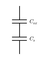
$$\begin{aligned} C_{gb}' &= \frac{C_s' C_{ox}'}{C_s' + C_{ox}'} \\ &= \left(\frac{1}{C_s'} + \frac{1}{C_{ox}'}\right)^{-1} \end{aligned}$$Therefore, the equivalent circuit of the MOS capacitor is one with $C_{ox}'$ and $C_s'$ in series.
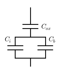
Since $C_s'$ is the summation of $C_i'$ and $C_b'$, it can be broken into the parallel combination of its two components.
Real devices have added parasitics such as the resistance between the surface and the body terminal.
10.0 References 
- Physical Properties of Semiconductors archive hosted by the Ioffe Physico-Technical Institute, http://www.ioffe.ru/SVA/NSM/Semicond/.
- R. van Langevelde, A. Scholten, and D. Klaassen, “Physical Background of MOS Model 11,” Philips Electrons, N.V., Tech. Rep. 2003/00239, 2003.
- Y. Tsividis, Operation and Modeling of the MOS Transistor. McGraw-Hill, 1987.
- E. Nicollian and J. Brews, MOS (Metal Oxide Semiconductor) Physics and Technology. Wiley-Interscience, 2003.
- R. F. Pierret, Advanced Semiconductor Fundamentals. Prentice Hall, 2003.
- T. Chen and G. Gildenblat, “Analytical approximation for the MOSFET surface potential,” Solid-State Electronics, vol. 45, no. 2, pp. 335 – 339, 2001.
Download this post's IPython notebook here.
Comments !